Discover the hidden causes of electronic failures - professional analysis, full explanation.
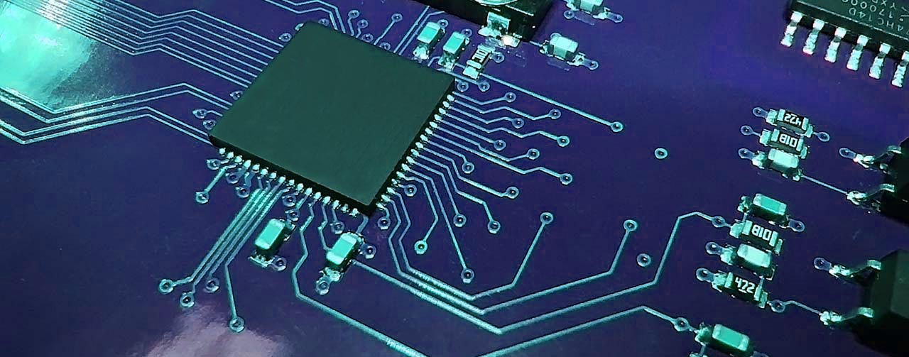
We specialize in comprehensive analysis of electronics failures, focusing on precise location of the issue and identification of possible causes. By employing various techniques, ranging from simple electrical measurements to a scanning electron microscopy (SEM/EDS), we are able to conduct precise analysis. Subsequently, we recommend solutions to product design or production process optimization to enhance the device reliability.
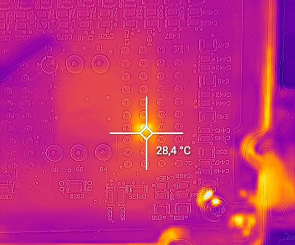
We employ various tools, including both standard methods and our own, based on years of experience, advanced failure location detection techniques.

Detailed investigations ranging from simple optical microscopy and electrical measurements to advanced materials analysis using SEM/EDS (scanning electron microscopy/energy dispersive X-ray spectroscopy).
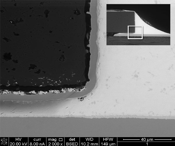
A failure can be caused by a variety of reasons, which can be related to the product design, production process, environmental impact or misuse of the product. We identify these based on previously collected data.
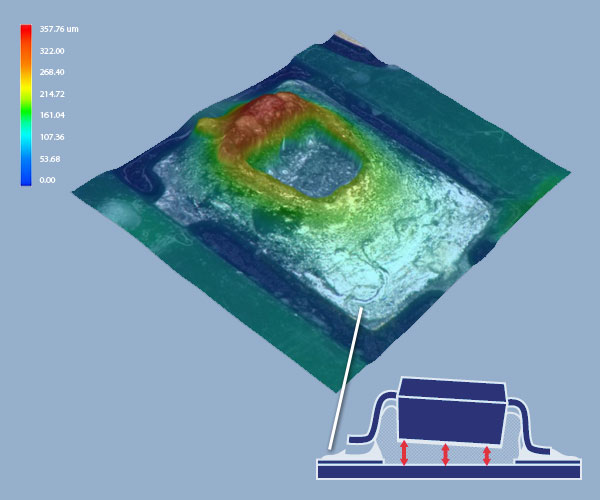
Develop a list of recommended corrective actions to address the causes of the problem. The actions may involve changes in the design of the device or improvements in the manufacturing process.
